
 Product
 Brand
Brand Articles
 Tools
Tools
Introduction to Photonic Integrated Circuits and PIC Technology
Silicon photonic integrated circuits and lasers
Originally published in 2020, this article has been updated to reflect the latest technological advancements, market trends, and breakthroughs in the rapidly evolving field of photonic integration as of October 2025.
With the relentless demand for higher bandwidth and energy efficiency, driven by the rise of artificial intelligence (AI), 5G networks, and large-scale data centers, the need to upgrade network infrastructure at lower costs and with reduced energy consumption has never been more critical. Similar to the revolution sparked by electronic integrated circuits, the maturation of photonic integrated circuit (PIC) technology is catalyzing another profound transformation in optical information technology. PICs promise to deliver unprecedented performance, scalability, and efficiency by manipulating light on a microchip.
Catalog
I. Classification of Photonic Integrated Circuit Platforms
The choice of substrate material is fundamental to a PIC's performance, cost, and application range. Each platform offers a unique set of advantages and challenges. The industry has moved beyond monolithic classifications to a platform-based approach.

| Platform | Key Characteristics & Advantages | Limitations & Challenges | Primary Applications |
|---|---|---|---|
| Silicon (Si) | Leverages mature CMOS manufacturing for low-cost, high-volume production. High refractive index contrast allows for dense integration and small device footprints. | Indirect bandgap makes it inefficient for light generation, requiring hybrid integration of III-V materials for lasers. | Data center transceivers, co-packaged optics, LiDAR, quantum computing. |
| Indium Phosphide (InP) | Direct bandgap material allows for monolithic integration of active components like lasers, amplifiers, modulators, and detectors. Enables true "all-in-one" chips. | More expensive and complex fabrication compared to silicon. Wafers are smaller, limiting scalability. | High-performance telecommunications, 5G networks, high-speed data links. |
| Silicon Nitride (SiN) | Extremely low propagation loss across a broad transparency window (visible to mid-IR). Excellent for high-Q resonators and passive components. | Lacks native light generation and high-speed modulation capabilities, often used in hybrid approaches with other materials. | Biosensing, LiDAR, nonlinear photonics, AR/VR, quantum networks. |
| Lithium Niobate (LiNbO₃) | Superior electro-optic properties for high-speed, high-linearity modulators. Strong nonlinearity for frequency conversion. | Historically difficult to process, but thin-film lithium niobate (TFLN) is changing the game. Birefringence can be a challenge. | High-bandwidth modulators, quantum photonics, RF-over-fiber. |
| Silicon-Germanium-Tin (SiGeSn) | A 2024-2025 breakthrough. Enables the first Group IV electrically pumped lasers directly on silicon, solving a major challenge for silicon photonics. | Emerging technology, requires cryogenic temperatures for operation currently. Still in the research and development phase. | Future on-chip light sources for fully integrated silicon PICs. |
II. Industry Demands & Market Growth for PICs (2025)
The demand for PICs has exploded since 2020, driven by exponential data growth and the need for faster, more efficient processing. The global PIC market was valued at approximately $17.93 billion in 2025 and is projected to soar to $97.62 billion by 2034. The silicon photonics segment alone is expected to maintain a compound annual growth rate (CAGR) of 20% over the next decade.
Key drivers include:
AI and Machine Learning: The insatiable data transfer requirements of AI training and inference workloads are pushing data centers towards optical interconnects. Collaborations like the one between STMicroelectronics and Amazon Web Services (AWS) to produce silicon-germanium PICs for AI infrastructure highlight this trend.
Telecommunications and 5G: The rollout of 5G and the upcoming 6G standards require massive upgrades to backhaul and fronthaul networks, where high-speed, low-latency PIC-based transceivers are essential.
Emerging Applications: Significant growth is also anticipated in applications like automotive LiDAR, advanced biosensors for point-of-care diagnostics, and quantum computing, where PICs provide the only viable path to scaling complex optical systems.
III. Development Status & Recent Breakthroughs in PIC Technology
The period between 2020 and 2025 has been marked by significant breakthroughs that are solving long-standing challenges in the field.
The "Last Missing Piece" for Silicon Photonics
In a landmark achievement published in late 2024, an international research team developed the first electrically pumped continuous-wave semiconductor laser made entirely from Group IV elements (silicon-germanium-tin). This laser, grown directly on a standard silicon wafer, is compatible with CMOS manufacturing processes. While it currently operates at cryogenic temperatures, it represents a critical step towards creating a fully integrated, low-cost light source for silicon PICs, a challenge that has been pursued for decades.
Maturation of Hybrid Integration and Co-Packaged Optics
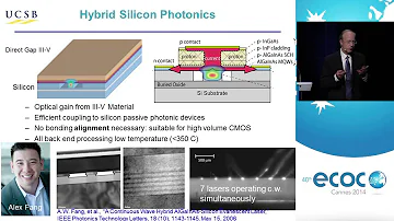
Hybrid integration, which combines the strengths of different material platforms (e.g., bonding InP lasers onto silicon PICs), has become a mainstream, commercially viable solution. This has led to the rise of co-packaged optics (CPO), where optical I/O is integrated directly with the main processing chip (like a CPU or GPU) in the same package. This approach drastically reduces power consumption and latency by shortening the electrical path, a critical factor for high-performance computing and AI clusters. Companies like Ayar Labs, which secured $155 million in funding, are at the forefront of this transition.
IV. Future Development Directions for PIC Technology
Continued Research on Silicon-Based Large-Scale PICs
The industry is pushing towards higher levels of integration and performance. Research is focused on achieving room-temperature operation for Group IV lasers and scaling production to 300mm wafers. The goal is to create complex systems-on-a-chip that combine logic, memory, and photonics, enabling ultra-high-bandwidth communication at the chip level. This is seen as essential for next-generation AI accelerators and processors.
Expansion into New Wavelengths and Applications
While data communications primarily use near-infrared wavelengths, there is growing interest in using PICs for a wider range of the electromagnetic spectrum. Silicon nitride, with its broad transparency, is enabling applications in the visible spectrum for AR/VR displays and biosensors, and extending into the mid-infrared for environmental sensing and medical diagnostics.
The Role of PICs in Optical Transport Networks (OTN)
High-speed transmission and dense integration are core strengths of PICs. In the context of Optical Transport Networks (OTN), PICs are enabling a new generation of hardware that combines high-speed interfaces with advanced networking and scheduling capabilities. The OTN market is robust, valued at over $25 billion in 2024 and projected to grow steadily. PIC-enabled OTN devices achieve high-quality, high-speed link grooming while improving network transparency and simplifying end-to-end management.

V. 2025 Update Summary
This article was originally published in 2020. This 2025 update incorporates significant industry developments:
Market Growth: Updated market data reflects the explosive growth driven by AI, with projections now reaching nearly $100 billion by 2034.
Technological Breakthroughs: The creation of the first Group IV electrically pumped laser on silicon is a major addition, solving a long-standing problem.
Material Platforms: The classification has been updated to a platform-based view, including modern materials like Silicon Nitride, TFLN, and the new SiGeSn alloys.
Industry Drivers: The role of AI and co-packaged optics as primary market drivers has been emphasized.
Recommended Articles:
Introduction to Voltage Stabilizer
LED Driver: Function, Types, and Application
 UTMEL
UTMEL
We are the professional distributor of electronic components, providing a large variety of products to save you a lot of time, effort, and cost with our efficient self-customized service. careful order preparation fast delivery service
1.What are photonic integrated circuits used for?
It is used in fibre-optic communication to make Externally Modulated Lasers (EML) which has a combination of a distributed feedback laser diode and an electro-absorption modulator on a single Indium-Phosphide [InP] chip.
2.What photonic IC contains?
In an electronic chip, electron flux passes through electrical components such as resistors, inductors, transistors, and capacitors; in a photonic chip, photons pass through optical components such as waveguides (equivalent to a resistor or electrical wire), lasers (equivalent to transistors), polarizers, and phase.
3.What is photonic semiconductor?
Introduction Optoelectronics is a branch of Photonics Science concerns with devices and systems that combine both electronic devices where information is carried among electrons and holes (generation and recombination) and photonic devices.
4.What are photonic devices?
Photonic devices are components for creating, manipulating, or detecting light. This can include laser diodes, light-emitting diodes, solar and photovoltaic cells, displays, and optical amplifiers.
5.Why are integrated circuits important?
The advent of the integrated circuit revolutionized the electronics industry and paved the way for devices such as mobile phones, computers, CD players, televisions, and many appliances found around the home. In addition, the spread of the chips helped to bring advanced electronic devices to all parts of the world.
 Discovering New and Advanced Methodology for Determining the Dynamic Characterization of Wide Bandgap DevicesSaumitra Jagdale15 March 20242673
For a long era, silicon has stood out as the primary material for fabricating electronic devices due to its affordability, moderate efficiency, and performance capabilities. Despite its widespread use, silicon faces several limitations that render it unsuitable for applications involving high power and elevated temperatures. As technological advancements continue and the industry demands enhanced efficiency from devices, these limitations become increasingly vivid. In the quest for electronic devices that are more potent, efficient, and compact, wide bandgap materials are emerging as a dominant player. Their superiority over silicon in crucial aspects such as efficiency, higher junction temperatures, power density, thinner drift regions, and faster switching speeds positions them as the preferred materials for the future of power electronics.
Read More A Comprehensive Guide to FPGA Development BoardsUTMEL11 September 202520515
This comprehensive guide will take you on a journey through the fascinating world of FPGA development boards. We’ll explore what they are, how they differ from microcontrollers, and most importantly, how to choose the perfect board for your needs. Whether you’re a seasoned engineer or a curious hobbyist, prepare to unlock new possibilities in hardware design and accelerate your projects. We’ll cover everything from budget-friendly options to specialized boards for image processing, delve into popular learning paths, and even provide insights into essential software like Vivado. By the end of this article, you’ll have a clear roadmap to navigate the FPGA landscape and make informed decisions for your next groundbreaking endeavor.
Read More 800G Optical Transceivers: The Guide for AI Data CentersUTMEL24 December 202510896
The complete guide to 800G Optical Transceiver standards (QSFP-DD vs. OSFP). Overcome supply shortages and scale your AI data center with Utmel Electronic.
Read More The 2026 Engineer’s Guide: Choosing the Right MCU for Your Next IoT & New Energy ProjectUTMEL30 April 2026893
A comprehensive comparison of 2026's leading MCUs from ST, NXP, and Microchip across power efficiency, processing performance, connectivity, and ecosystems to help engineers select the optimal chip for next-gen IoT and new energy projects.
Read More AI Server Components: Engineering Next-Gen Data Center Hardware for 100kW RacksUTMEL15 May 2026429
The transition from traditional enterprise IT to AI-driven workloads has rendered legacy data center hardware obsolete, forcing infrastructure planners to re-engineer server components for extreme thermal environments.
Read More
Subscribe to Utmel !
![UCC5310MCDR]() UCC5310MCDR
UCC5310MCDRTexas Instruments
![1EDI20H12AHXUMA1]() 1EDI20H12AHXUMA1
1EDI20H12AHXUMA1Infineon Technologies
![1EDI60H12AHXUMA1]() 1EDI60H12AHXUMA1
1EDI60H12AHXUMA1Infineon Technologies
![1EDI30I12MFXUMA1]() 1EDI30I12MFXUMA1
1EDI30I12MFXUMA1Infineon Technologies
![UCC21220DR]() UCC21220DR
UCC21220DRTexas Instruments
![HCS201T-I/SN]() HCS201T-I/SN
HCS201T-I/SNMicrochip Technology
![ADATE305BSVZ]() ADATE305BSVZ
ADATE305BSVZAnalog Devices Inc.
![AD9172BBPZ]() AD9172BBPZ
AD9172BBPZAnalog Devices Inc.
![ADUM4223CRWZ]() ADUM4223CRWZ
ADUM4223CRWZAnalog Devices Inc.
![FM33256B-G]() FM33256B-G
FM33256B-GCypress Semiconductor Corp


